|
TA17B
VLSI & ASICS Digital devices
Testing
• Processors and peripheries
• Memories
• Logic arrays
• TTL logic devices
Test Groups Architectur
• 48 bidirectional test signals
• Data rate up to 10 MHz
• Hardware test evaluation in the input
mode
- Expected data
stored in the
output
channel
- Input data
compared with the
expected data
- Fail marks on the
input vectors
stored
- 10-bit fail
events counter
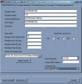
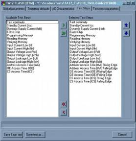
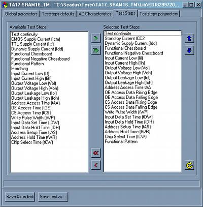
Screenshots |
| Parameters |
| Parameters |
Group
0 |
Group
1 .. 5 |
| Signals
Number |
8
bidirectional |
| Pattern
Out Depth |
1048
(Standard)
32768 (max) |
| Pattern
In Depth |
1048
(Standard)
32768 (max) |
| Direction
Control |
Single
(In or Out) |
Common
(In or Out) |
| Output
Timing |
Single
(Start/Stop) |
Common
(Start/Stop) |
| Input
Timing |
Common
(Load Point) |
| Format
Control |
common |
| Output
Format * |
return-to-zero
return-to-one
surround-by-complement
non-return |
| Input
Format |
Data |
data
fail marks
fail number
(0..65535) |
| FIFO
Unit Control |
Reset
and Retransmit |
| FIFO
Unit Flags |
Empty
and Full |
| Synchronization |
Independent
In and Out |
| Output
Low Level |
0.3
V .. 5.5 V |
| Output
High Level |
0.3
V .. 5.5 V |
| Input
Threshold |
0.3
V .. 5.5 V |
| Timing
Range |
255
ns or 1275 ns |
| *
for all pins in the group |
|